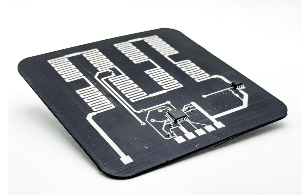
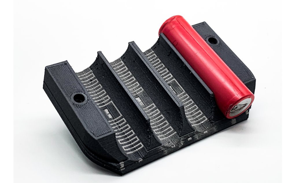
3D printed electronics have advanced with news that nScrypt‘s research arm, Sciperio has demonstrated a significant improvement in the performance of conformal 3D Printed Circuit Structures (PCSs). nScrypt says this was possible due to its high-precision Factory in a Tool.
The research was geared towards enhancing 3D manufactured conductive traces and vias, the small openings in a PCS, to boost overall yield and performance adjustability. The team put these improvements to practical use by printing a circuit that featured conformal heating elements, which have versatile applications such as wearable technology, electronic devices, and heating systems.
“The lower resistance traces we made with nScrypt’s Factory in a Tool open the door for higher-power conformal PCS circuitry. Our improved via yields also allow for increased circuit density. These advances bring the performance of PCSs closer to that of traditional PCBs and are an important step toward high-performance electrically functional devices of virtually any shape,” says Ken Church, CEO of nScrypt and Sciperio.

Stacked conductive layers and Via-Filling techniques
According to the study, utilizing stacked conductive layers for traces resulted in a considerable reduction in resistance compared to single-stacked traces. As the number of layers increased, the resistance steadily decreased, with a 92% reduction observed from layer 1 to layer 7 without oven curing. This in turn exhibited substantially lower resistance than a single-layer trace of the same height. The extra height of the stacked trace can be counterbalanced by integrating the trace into the 3D-manufactured circuit structure, as per the study.
In addition, a technique for via-filling was devised, using the nScrypt SmartPump to coat via walls with a conductive substance via a vacuum extraction method. Via-Filled is an electronic manufacturing process that entails filling small holes or vias on a printed circuit board (PCB) with conductive material.
As per the study, the vacuum evacuation technique yielded satisfactory results in connecting 49 out of 50 vias, with an average resistance of 4.8m? and a standard deviation of 0.47m?. The team then implemented these advancements in a prototype PCS that featured conformal 3D printed heating elements enabled by stacked traces. The heating elements were 3D printed with different numbers of stacked conductive layers per section, demonstrating the adjustability of resistance without modifying trace widths.

Advances in 3D printed electronics
InnovationLab, a German firm specializing in 3D printing for electronics, created a cost-effective and eco-friendly approach to producing Printed Circuit Boards (PCBs). As part of the EU Horizon 2020 project ‘SmartEEs2,’ the process facilitates the creation of copper circuits that can be soldered, utilizing less energy than conventional methods and eliminating the use of hazardous etchants. In collaboration with partner ISRA, the company has developed prototype PCBs that could form the foundation for next-generation flexible and wearable electronics.
BotFactory, a specialist in circuit board fabrication, was awarded a contract by the U.S. Air Force (USAF) to create an entirely automated desktop 3D printer for electronics. The company’s engineers were developing a system as part of the USAF’s AFWERX program that can produce and assemble PCBs on-site and whenever required. In-house PCB manufacturing has the potential to save the USAF millions of dollars annually in procurement expenses while significantly reducing lead times in the aerospace prototyping process.
What does the future of 3D printing for the next ten years hold?
What engineering challenges will need to be tackled in the additive manufacturing sector in the coming decade?
To stay up to date with the latest 3D printing news, don’t forget to subscribe to the 3D Printing Industry newsletter or follow us on Twitter, or like our page on Facebook.
While you’re here, why not subscribe to our Youtube channel? Featuring discussion, debriefs, video shorts, and webinar replays.
Are you looking for a job in the additive manufacturing industry? Visit 3D Printing Jobs for a selection of roles in the industry.
Featured image shows 3D printed circuit board. Image via nScrypt.
Post Disclaimer
The information provided in our posts or blogs are for educational and informative purposes only. We do not guarantee the accuracy, completeness or suitability of the information. We do not provide financial or investment advice. Readers should always seek professional advice before making any financial or investment decisions based on the information provided in our content. We will not be held responsible for any losses, damages or consequences that may arise from relying on the information provided in our content.


